|
Terms Fido-Cad.
The Fido-Cad provides a wide range of content libraries to housing most used.
With using these libraries can achieve virtually any circuit.
The preliminary notions are needed:
- Setting the working environment.
- Concept layer
- Using the zoom
- Content Libraries
Inserting objects and thickness selection
Let's see in detail what to do:  On desktop once installed Fido-Cad will be an icon to launch, by Double-click
the program starts by presenting the Splasc (product name) shown in the drawing
below. On desktop once installed Fido-Cad will be an icon to launch, by Double-click
the program starts by presenting the Splasc (product name) shown in the drawing
below.
 After missing the window presentation we will be in front of a room that reminds
us vaguely Autocad.
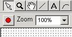
Here's what the simple Toolbar design software.
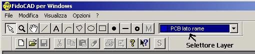 If we are interested in developing the PCB (printed circuit) we ensure that the
Layer Selector (selector or work plan) is set to "PCB copper side" even if by
default it will lead to "scheme" pointing to a black instead of blue.
The menu Layer allows us to divide the work on several levels, so that the
computer is being printed able to separate the tracks from the printing on the
components that do not obviously must appear in the master.
The master can be printed with a laser printer on glossy paper specification.
In order to avoid damaging the roller is well do not try to print on glossy
paper for copiers, paper specification is still readily available at any
stationery store.
The Fidocad provides less than 16 Layer, of which the first four are predefined,
they are:
- Scheme (Black)
- PCB side copper (blue)
- PCB side components (green)
- Serigraphs (bluish in color)
Once we set the Layer proceed to create the new worksheet using the control file
followed by again. We will propose three options shown in the figure follows:
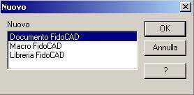
the correct item is new -> document FidoCad
The other two items to create new objects to be included such as new components,
or if there is provided by third parties (or because we found on the Internet)
entire libraries.
For the first experiments, the libraries provided the default is more than
satisfactory.
Once the new document FidoCad appear the grid work that is already prepared to
step choir. The zoom control on the other hand, is a very high magnification,
then you should take him to the maximum value of 100% or 150% in order to have a
vision of the easier routes to run.
Inserting, moving, moving relative rotation of the object.
- If you click on the toolbar hand, We center the inserted object (Macro)
in the monitor or move around the sheet work on the window displaying a portion
of the monitor but there is no relative motion of the macro (or component) than
the other components.
- If you click on the toolbar white arrow will can move the macro in the
sheet while leaving the firm other items previously entered.
- To rotate an object at point prepared and indicated by the blue square
just after selecting it with the frecetta white press the letter R or CTRL + R.
FIDO CAD libraries.
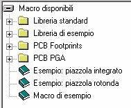
On the right side of the environment FidoCAD there is the tree of the libraries
contain the macro expansion of the objects that we use in our circuit.
The tree of standard libraries without expand the branches has the appearance
shown in the figure.
In order to start develop our first base expand the branch PCB Footprint
(translated English mean impression).
Obviously, in order to develop a printed circuit we need to know the dimensions
and physical measurements components, or their "footprint".
 As we can see on this folder find almost everything that we can serve from
simple resistance divided into different physical dimensions depending on the
ability to dissipate power, the generic Dil integrated circuits (dual in
line with various amounts of legs), The chips power SIP Clippwatt, multiwatt,
etc.. even up to possibility of including a broad range of integrated SMD (Surface Mountaga device). As we can see on this folder find almost everything that we can serve from
simple resistance divided into different physical dimensions depending on the
ability to dissipate power, the generic Dil integrated circuits (dual in
line with various amounts of legs), The chips power SIP Clippwatt, multiwatt,
etc.. even up to possibility of including a broad range of integrated SMD (Surface Mountaga device).
The first item Cards & Co are the measurements of standard autoimprimenti
whiskers, usually tends to use the measure at 100 x 160 mm, and play in it
more copies of the same circuit.
This optimizes the cost of production.
Also under this heading are the holes for the mounting screws on the
standard diameter 3MA.
It is important to know the difference between Wide and narrow of the plots.
The first when we use our homemade PCB is not too dense, then the slopes larger ensure that they are not destroyed during the drilling.
Also useful are browsing the tree, but keep in mind that FidoCAD also allows you
to draw the wiring diagram. Under Standard library not find the imprint of
integrated or discrete components, but their graphic symbol that we can use to
document schemas. carry some items such as example.
The terminal blocks.
The printed circuit boards require points of access and egress to and from other
circuit boards or machines electric users in general.
The screw terminals are to be printed characterized by a standard pitch of 5 mm
while their overall physical PCB cover a wide strip of about 11 mm.
The FidoCAD does not provide in the footprint of the standard library so we have
two screw terminals possible solutions, the first is to create a custom macro
(but This goes beyond the basics), the second is more of a trick, In fact,
knowing that the distance between the spots is equal to that of a polyester
capacitor 5mm Box step we can use this component like a screw terminal.
Obviously, using this technique solve the problem of distance between the holes
but not the footprint physical.
To understand how much PCB area will covered by the terminal will need to
overturn it in a perpendicular same capacitor.
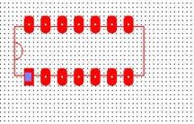
Terminals for multi-point connection iterate the overlap of the two pitches
capacitor to the right or left.
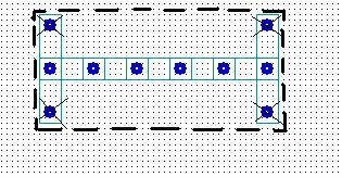
The picture is the estimated footprint of a screw terminal block of 6 connection
points, ITER is the size of a capacitor polyester Box 5 mm pitch.
Those places are only vertically to estimate the physical footprint and then
dotted area (which will not appear in your PC) should not be included other
components.
If some other device then invaded the area at the end of work terminal can not
be inserted because superimposed on it.
Zoom
For a correct view of all is should begin work by placing the zoom value of
100%.
We follow this procedure to begin the job properly:
- From diagram identify and count all the components.
- From Library PCB Footprint taken all the components in question, missing
ones we got just the physical footprint using other equipment proceed on a
distributed new document fidocad all these documents.
- Distribute the components on the sheet in a way that it seems a priori more
compact and useful to trace the tracks begin by recalling that for Our
equipment is good to use home runs with a thickness of between 7 and 9 points.
Dimensioning of the thickness of slopes.
To correctly choose the thickness of the tracks we make a dash in a anywhere on
the page, then select the white arrow in "Select / Move" with which we do a
double click on the dash track.
A dialog selection invites us to select the most appropriate thickness.
As indicated previously, it is good that for the beginner slopes are not of
thickness less than 8 points.
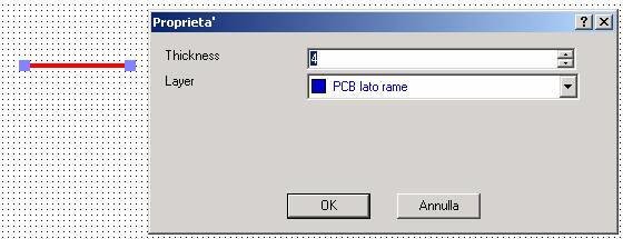
With the word Thickness is defined as the thickness in pixels of the section of
track.
Once you select a thickness will remain so until a new selection.
By default FidoCAD positioning initially in a thickness of 4 pixels as shown in
the figure, but this thickness as mentioned above should be for experienced
developers.
The minimization of copper corrode.
The dual purpose of not quickly saturate the solution of ferric chloride and to
maximize ground planes that reduce the induced currents and parasitic resistance
is used to maximize the thickness of the slopes.
A bottle of 1 liter chloride iron can be used for hundreds of copies of
electronic only if they adhere to the rule of minimization.
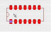
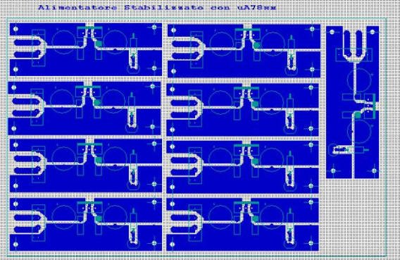
Let's see an example of images that represent the same circuit.
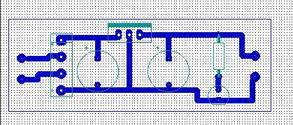
The power supply in the figure is correct and functioning, the tracks are of a
thickness of 10 pixels and the terminals have a width of 5 mm.
The pitches are reinforced with a size of 20 pixels in both circles.
We note that most the surface of the board is not committed to the slopes, then
the solution acid will remove a great deal of copper and then ensure effective
for a small number of samples.
The solution to this problem is to maximize the thickness of the slopes but this
can be done alone and Only after you have confidence that the circuit is choir,
In fact, once the scheme maximized the reading is more difficult.
It 'obvious that the same pattern appears more functional and more favorable
savings.
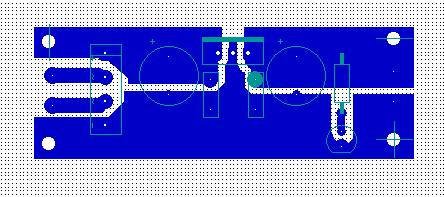
Multiplication of the specimens.
The minimum cost occurs when there is the maximization of the product at the
same use of raw material, it follows that if the same base 100 x 160 mm we can
introduce a large number of specimens of the same cost will be divided by the
number of specimens.
The designer must keep in mind this goal.
In the picture below we can see the finished product, or a regulated power
supply derived from metal cutting with scissors (shears, available at hardware
stores), one of the seven specimens seen in the PCB above. Note how important it
is to forecast the overall cooling fin.
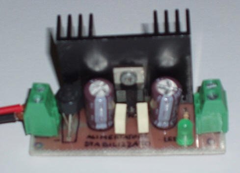
The size of the board is 65 mm x 25 mm. |