|
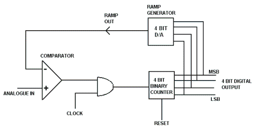
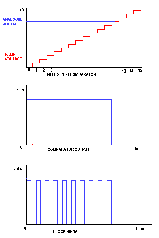
 At the start, the inverting input of the comparator is low and its output high. The AND gate is enabled. Clock pulses appear at the output of the gate and are counted by the UP counter when the counter is reset to zero. As the count increases, the ramp output voltage of the D/A converter rises. When the ramp voltage and the analogue voltage are the same, the output of the comparator goes low. This inhibits the AND gate and the count stops. The 4 bit number at the output, is the binary equivalent of the analogue input voltage. This process repeated continually.
 |