|
System Overview Figure 2.1 illustrates the basic components of the Personal Silent Alert System.

Figure 2.1 - Block diagram of the system
The TTY and the detector-transmitter unit are connected to separate phone jacks on the same line. When the ring sensor detects an incoming phone call, it activates the transmitter, which sends an RF signal to the receiver in the pager device. The receiver activates intermediate circuitry which drives the vibrating motor and thus alerts the user to the incoming call.
In this section we describe the design and implementation of the ring detector and its connection to the transmitter. We also describe the circuitry in the pager that connects the receiver to the vibrating motor.
Ring Detection And The RF Transmitter
The Telephone Line
We required an understanding of the signals and standards used in telephone communication in order to build the interface between the telephone line and the transmitter. Figure 2.2 shows the signals on a silent and a ringing telephone line.
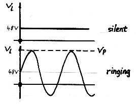
Figure 2.2 - Phone signals
When the line is silent, a DC voltage of Vl = 48 V is present. During ringing this voltage is superposed with a sine wave of considerably large amplitude. Often the ringing amplitude is 80 Vrms, which gives a peak voltage of Vp = 48 V +/- 1.4 * 80 V = {+160 V; -64 V}. Not all telephone companies use the same standard for their ring signals, so the amplitude and frequency can vary over a wide range.
A telephone line in use has a small DC voltage of approximately Vl = 4 V with a superposed current signal (from a voice, fax, or modem) which corresponds to a voltage change of up to 2 V in amplitude.
Note that neither the "RING" nor the "TIP" terminal of a telephone line can be grounded.
Ring Detection
In order to make our product compatible to every telephone ring standard, we used the amplitude of the line voltage to distinguish a ringing line from all other possible telephone line states. All telephone standards have one property in common: The peak voltage of a ringing line is significantly higher than the DC voltage for a silent line or a line in use. Using this approach the frequency of the ringing signal does not play a role in detecting a ring signal. Figure 2.3 shows the block diagram of the ring detector.
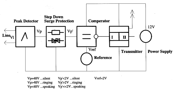
Figure 2.3 - Ring detector block diagram
 Figure 2.4 shows the circuit schematics for the ring detector.
The incoming voltage Vl comes from the telephone line and goes into a peak detector where the peak voltage is stored for 0.1 seconds. This duration is double the period of the lowest possible ringing frequency of 20Hz. The voltage Vp is the output of the peak detector. Vp is 48 V for a silent line, greater than 48 V for a ringing line, and much less than 48 V when the line is in use.
Voltage Vp is stepped down by the succeeding potential divider to a voltage Vp', where Vp' is about 2 V for the silent line, greater than 2 V for a ringing line, and much less than 2 V when the line is in use. Because of the inductance in the telephone line, high voltage peaks can occur if the current in the line changes rapidly. Such current changes can be caused by dialing, unplugging phones, driving mechanical ringers, and so forth. To protect our circuit from these undesirable high voltages, we implemented surge protection in our circuit.
After the peak voltage is stepped down, it is compared to the reference voltage Vref = 2 V. If Vp' is greater than 2 V the comparator triggers channel I of the transmitter, causing an RF signal to be sent.
The Transmitter
A purchased transmitter-receiver pair, RT300T & RF300, was used to send an alert on detection of an incoming call or a ringing doorbell. The vendor for the pair was Vistect Inc., P.O. Box 14156 Fremont, CA, 94539, (510) 651-1425. The transmitter operates at 318 MHz and provides up to three channels. According to the specifications given in its data sheet its transmission range is about 100 m. A security code can be set in the transmitter and the receiver to provide privacy and to prevent interference with other transmitter units using the same frequency.
The transmitter was packaged as a small hand-held device in a plastic case with two buttons to trigger either one or both of the channels. It was powered by a 12-V battery. In order to interface the transmitter to other circuitry, we bypassed the buttons with PNP transistors. Figure 2.5 shows this configuration in a simplified circuit diagram of our modified transmitter.
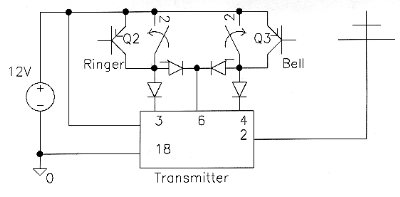
Figure 2.5 - Modified transmitter circuit schematic
With this modification, the transmission can be triggered by causing a small current (from 0.1 to 5 mA) to flow from the base of the PNP transistors to ground. While testing, we supplied this current by connecting the base to ground via a sufficiently large resistor (20 kOhm was sufficient).
The Power Supply
Since the transmitter unit is a stationary device it is convenient to use a wall plug for the power supply. We purchased a 9 V AC supply for this task. A bridge rectifier with a charging capacitor gives a DC voltage of 12 V.
Building The Transmitter Unit
We took the transmitter out of its case and soldered it to a prototype board. All other components except the transformer sit on this circuit board as well. One cable connects the circuit to the transformer; another cable, terminated in a standard phone terminator, connects the unit to a telephone socket. The circuit is housed in a purchased plastic case.
The RF Receiver and Pager Vibration
The pager consists of three main functional components: the RF receiver, some glue logic, and the vibrating motor. We purchased the RF receiver along with the RF transmitter, so its inner workings are not discussed here. The RF receiver has three outputs: Signal Enable, Data 1, and Data 2. Table 2.1 shows the values of these outputs for the transmitted signals.
Table 2.1
| | Off | Signal 1 | Signal 2 | | Signal Enable | Low | High | High | | Data 1 | High or Low | High | Low | | Data 2 | High or Low | Low | High |
The logic interfacing the receiver to the vibrating motor consists of two oscillators, an RC circuit, and a final inverting Schmitt trigger and transistor, as shown in Figure 2.6.

Figure 2.6 - Block Diagram of the pager unit Oscillator 1 produces a square wave with a period of 3 kHz; it is the source of the signal that drives the motor. The falling edge of this wave is delayed by the RC circuit, as shown in Figure 2.6, between the RC combination and the inverting Schmitt trigger. The inverting Schmitt trigger makes this wave square-cornered again, but now the duty cycle of the wave favors the low state. This final signal activates the motor. We adjusted the frequency of oscillator 1 and the time constant of the RC circuit so that the duty cycle is one ninth of the entire period. Since the power supply is at 9 V, this results in an average of 1 V being supplied to the motor. While the Data 1 signal is being received, oscillator 1 is turned on and the motor vibrates. This signal is allocated to the telephone ring detector, thus matching the vibration pattern of the pager to the standard ring pattern of 2 second on and 4 seconds off. While the Data 2 signal is being received, oscillator 2 is turned on. Oscillator 2 produces a square wave with a period of about 2 Hz. Its output is connected to the input of oscillator 1. Thus, it turns on and off oscillator 1 at a rate of roughly twice per second, producing a different vibration pattern. The circuit schematic for the glue logic is shown in Figure 2.7.

Figure 2.7 - Circuit schematic for the pager unit
Click for a larger version
The oscillators are implemented with two inverters in series and an RC pair which determines the period. Resistors R2 and R3 with capacitor C1 comprise the RC pair for oscillator 1 and resistor R11 with capacitor C5 make up the RC pair for oscillator 2. The AND gates IC1D and IC1C allow the oscillators to be turned on and off. The 1M-ohm resistors R4 and R12 prevent large current flows into the logic gates.
The output of the final inverting Schmitt trigger, IC2A, causes a current
through resistor R6, which controls the transistor. The transistor works as a
current amplifier to drive the motor and thus protects the logic circuitry from
large currents drawn by the motor. Notice that the OR gate in Figure 2.7 has
been implemented with two diodes. This allows us to use just two ICs: a quad-AND
gate and a hex-inverter. |